P N Junction Band Diagram: The Semiconductor Secret That Powers Modern Electronics - A) band alignment at the schottky junction of a metal/insulator
If you are searching about Extrinsic Semiconductors: Definition, Types, and Band Diagram you've visit to the right place. We have 35 Pictures about Extrinsic Semiconductors: Definition, Types, and Band Diagram like Circuit design EXP 03 P-N Junction Diode - Tinkercad, p-n junction band diagram - Knitive and also p-n Junction Diode and Characteristics of p-n Junction | Electrical4u. Here it is:
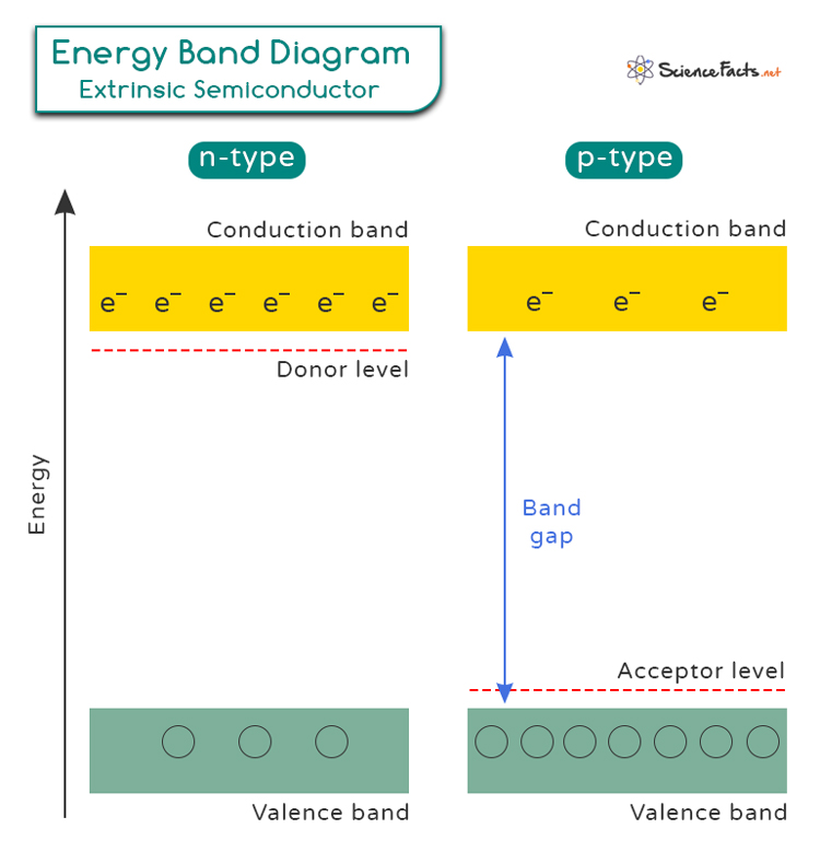
Extrinsic Semiconductors: Definition, Types, And Band Diagram
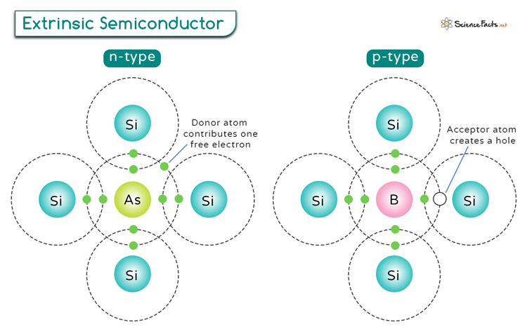 www.sciencefacts.net
Extrinsic Semiconductors: Definition, Types, and Band Diagram
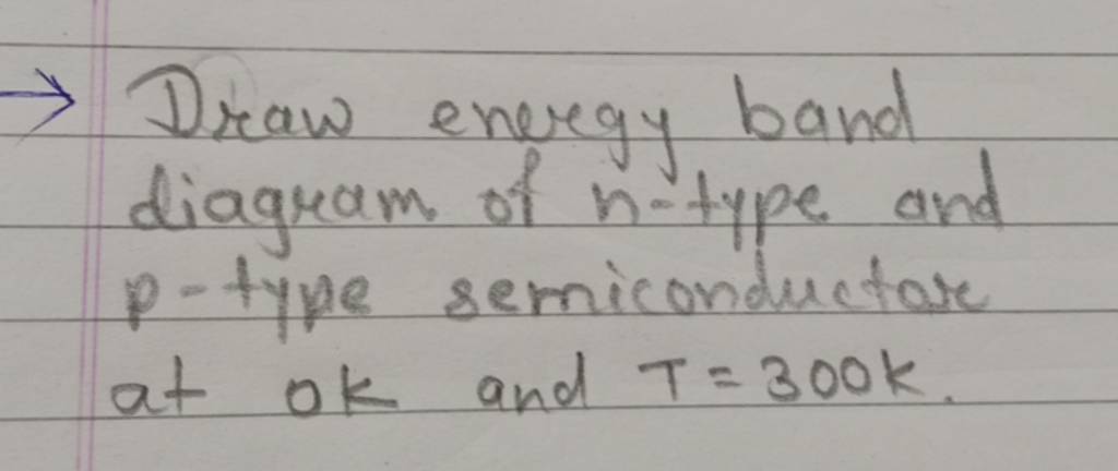
→ Draw Energy Band Diagram Of N -type And P-type Semiconductor At 0 K And..
 askfilo.com
→ Draw energy band diagram of n -type and p-type semiconductor at 0 K and..
Pin Photodiode Band Diagram Energy Diagram Of PN Junction With
 fity.club
Pin Photodiode Band Diagram Energy Diagram Of PN Junction With
P-Type Semiconductors: Uses, Benefits, And Key Applications
 www.agsdevices.com
P-Type Semiconductors: Uses, Benefits, and Key Applications
8. Band Structure Of Metal/p-type Semiconductor Schottky Junction At
 www.researchgate.net
8. Band structure of metal/p-type semiconductor Schottky junction at ...
Extrinsic Semiconductors: Definition, Types, And Band Diagram
 www.sciencefacts.net
Extrinsic Semiconductors: Definition, Types, and Band Diagram
P-n Junction Band Diagram - Knitive
 knitives.blogspot.com
p-n junction band diagram - Knitive
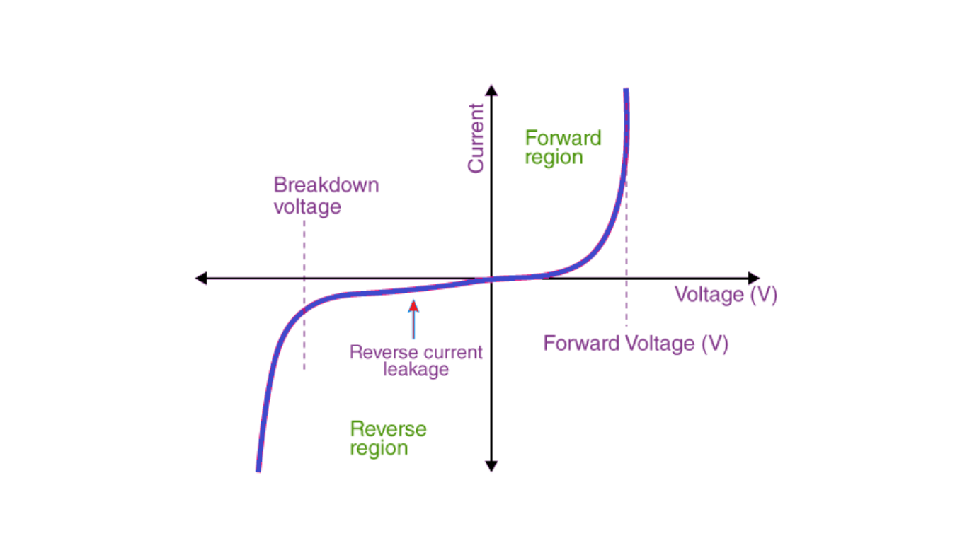
VI Characteristics Of P-N Junction Diode - Siliconvlsi
 siliconvlsi.com
VI Characteristics of P-N Junction Diode - Siliconvlsi
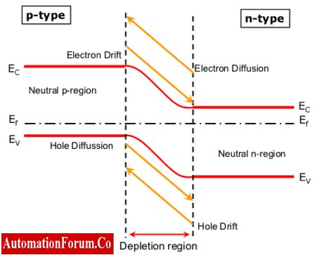
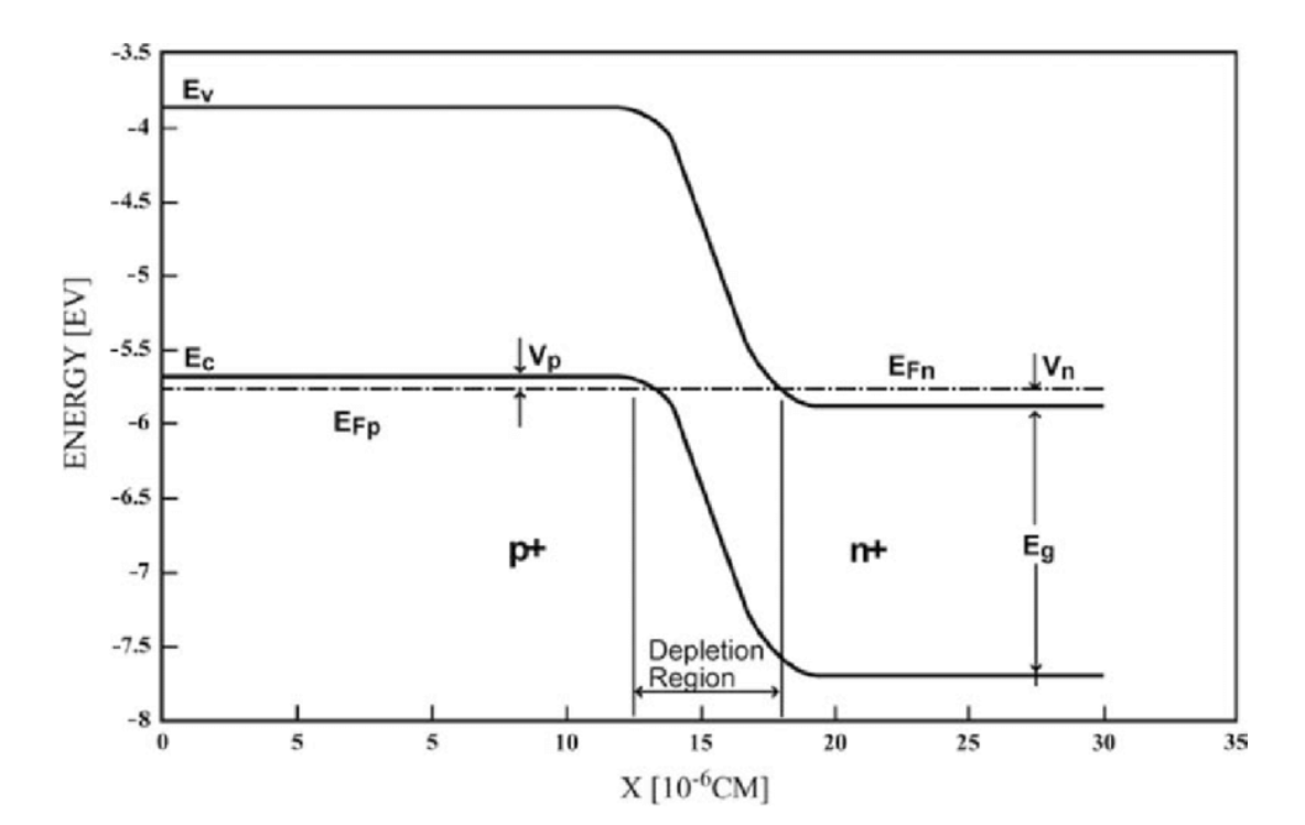
2: Band Diagram Of A P-n Junction Under Equilibrium, Showing Charge
2: Band diagram of a p-n junction under equilibrium, showing charge ...
Pn Junction Circuit Diagram
 www.circuitdiagram.co
Pn Junction Circuit Diagram
P-n Junction With Reversed Bias. Energy Band Diagram Is Also Shown
 www.researchgate.net
p-n junction with reversed bias. Energy band diagram is also shown ...
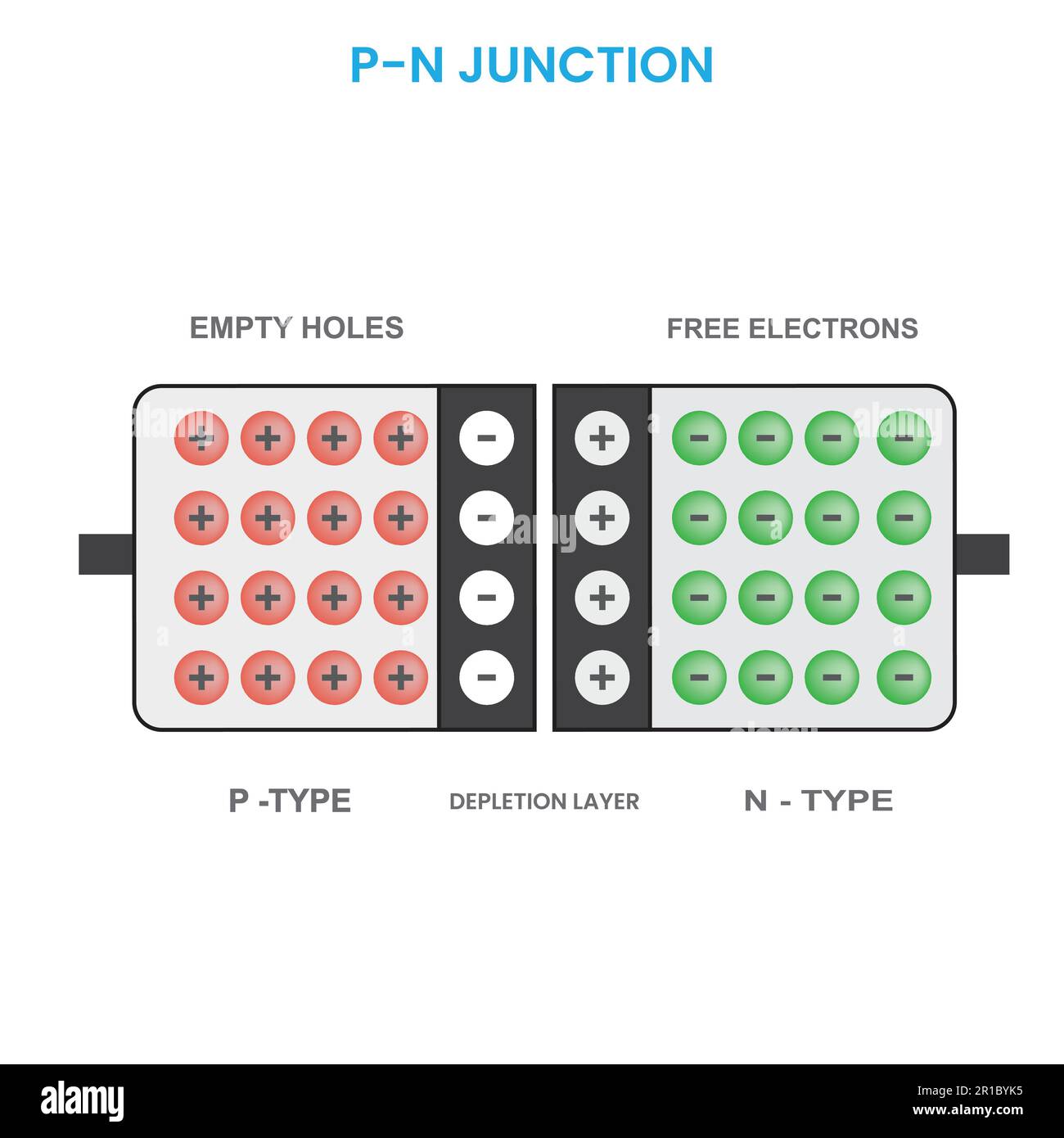
PN Junction Vector Illustration. P–n Junction Isolated On White
 www.alamy.com
PN junction vector illustration. p–n junction isolated on white ...
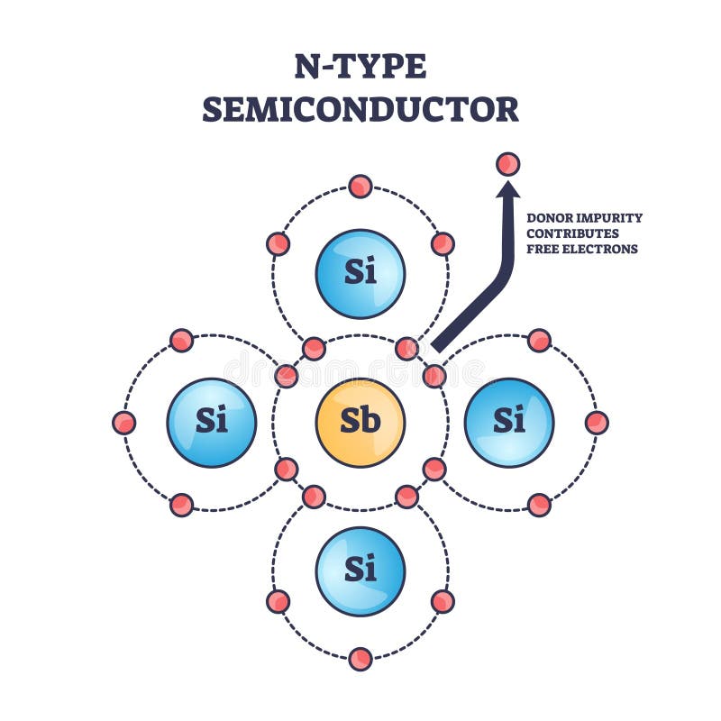
N-Type Semiconductor Diagram Shows Silicon Atoms And Free Electrons
 www.dreamstime.com
N-Type Semiconductor Diagram Shows Silicon Atoms and Free Electrons ...
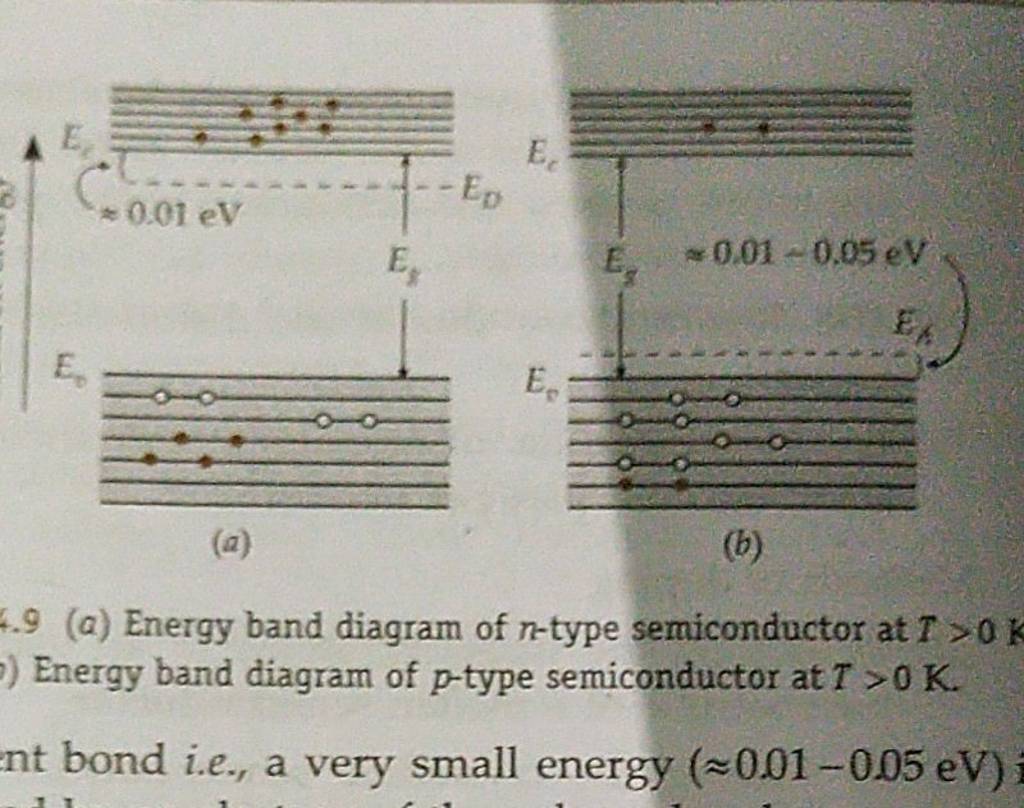
4.9 (a) Energy Band Diagram Of N-type Semiconductor At T>0k Energy Band D..
 askfilo.com
4.9 (a) Energy band diagram of n-type semiconductor at T>0k Energy band d..
P-n Junction Band Diagram - Knitive
 knitives.blogspot.com
p-n junction band diagram - Knitive
Intrinsic Semiconductor: Definition, Current, & Energy Band
 www.sciencefacts.net
Intrinsic Semiconductor: Definition, Current, & Energy Band
LED Working Principle, With Details For The Semiconductor P-N Junction
 www.researchgate.net
LED working principle, with details for the semiconductor P-N junction ...
P-n Junction Band Diagram - Knitive
 knitives.blogspot.com
p-n junction band diagram - Knitive
10 Astonishing Facts About P-n Junction - Facts.net
 facts.net
10 Astonishing Facts About P-n Junction - Facts.net
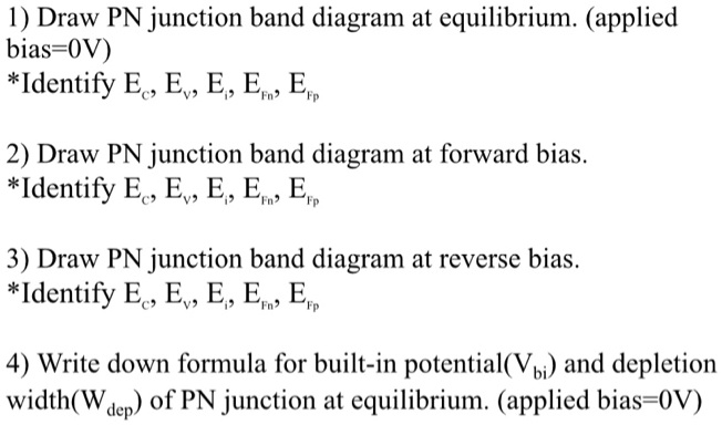
SOLVED: 1) Draw PN Junction Band Diagram At Equilibrium. (applied Bias
 www.numerade.com
SOLVED: 1) Draw PN junction band diagram at equilibrium. (applied bias ...
(A) Band Diagrams Of An N-type Semiconductor And Metal Before Contact
 www.researchgate.net
(A) Band diagrams of an n-type semiconductor and metal before contact ...
A) Band Alignment At The Schottky Junction Of A Metal/insulator
 www.researchgate.net
a) Band alignment at the Schottky junction of a metal/insulator ...
Simplified Electron Energy Band Diagram Of A Model Semiconductor Sample
 www.researchgate.net
Simplified electron energy band diagram of a model semiconductor sample ...
What Is P Type Semiconductor? – Energy Diagram & Conduction
 electronicslesson.com
What is P Type Semiconductor? – Energy diagram & Conduction
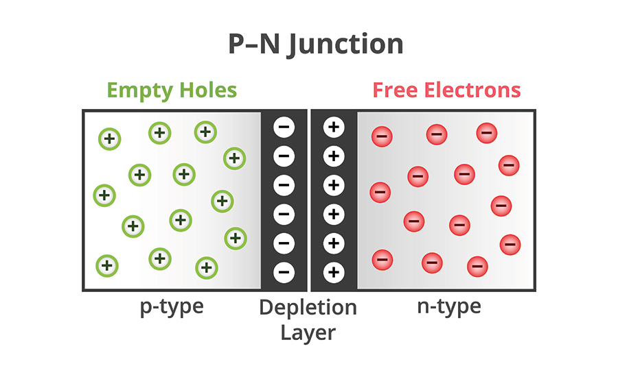
P-N Junction
 www.physics-and-radio-electronics.com
P-N junction
Energy-band Diagram For The Metal-semiconductor Junction (Schottky
 www.researchgate.net
Energy-band diagram for the metal-semiconductor junction (Schottky ...
P-n Junction Diode And Characteristics Of P-n Junction | Electrical4u
 www.electrical4u.com
p-n Junction Diode and Characteristics of p-n Junction | Electrical4u
Ferroelectric Tunnel Junction Band Diagram At Sophie Clarkson Blog
 storage.googleapis.com
Ferroelectric Tunnel Junction Band Diagram at Sophie Clarkson blog
Circuit Design EXP 03 P-N Junction Diode - Tinkercad
 www.tinkercad.com
Circuit design EXP 03 P-N Junction Diode - Tinkercad
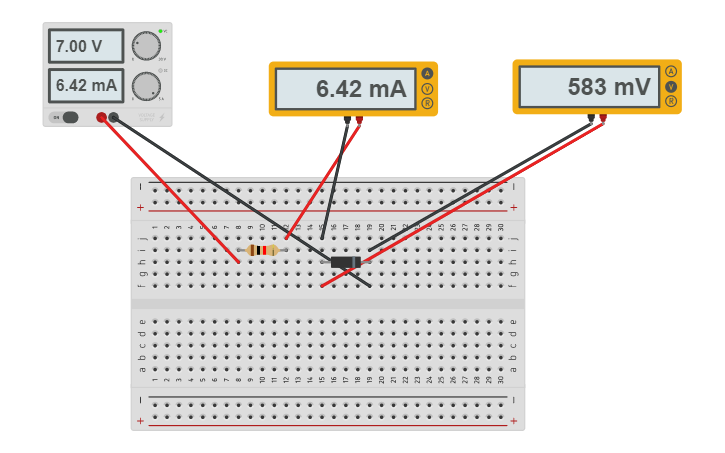
Solved The Energy Band Diagram Of A P-n Junction Under | Chegg.com
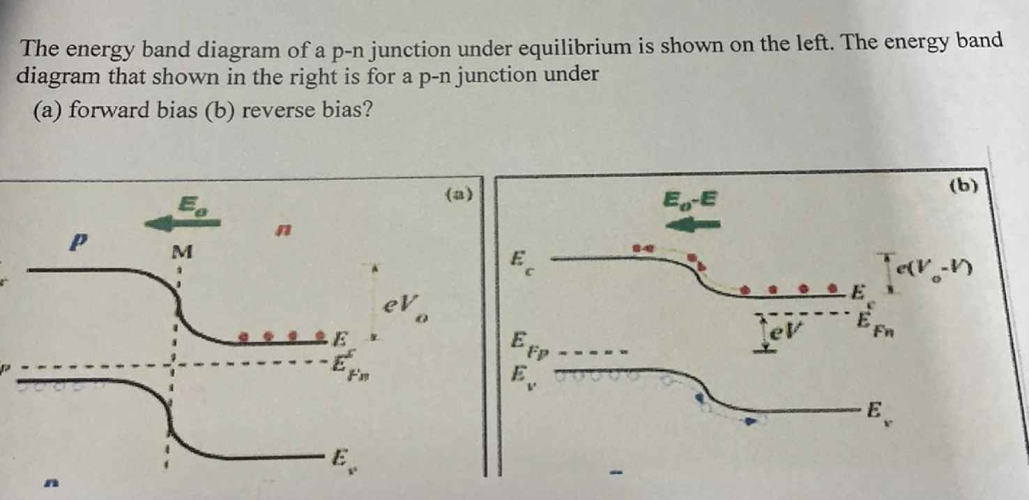 www.chegg.com
Solved The energy band diagram of a p-n junction under | Chegg.com
Potential Diagram Of The P-n Junction Solar Cell In Thermodynamic
 www.researchgate.net
Potential diagram of the p-n junction solar cell in thermodynamic ...
The Energy Band Diagram Of A Metal/ N -type Semiconductor And A Metal
 www.researchgate.net
The energy band diagram of a metal/ n -type semiconductor and a metal ...
Ace Tips About What Is The Band Gap Range Of A Semiconductor Blog
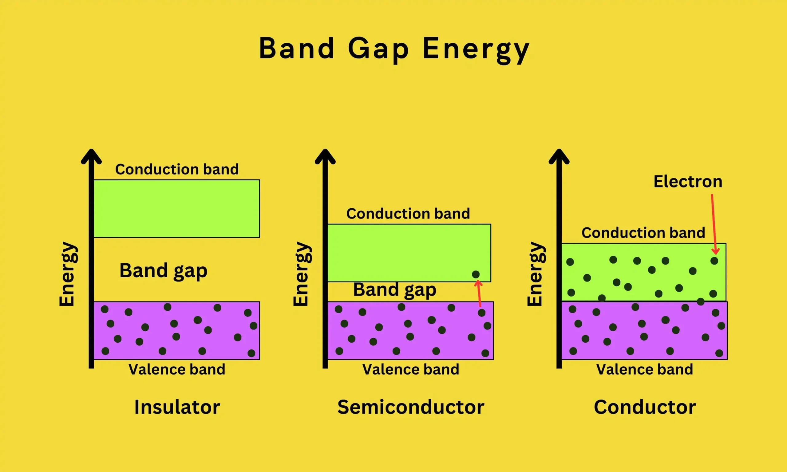 bethbourdon.com
Ace Tips About What Is The Band Gap Range Of A Semiconductor Blog ...
Solved The Band Diagram Of An Abrupt Pn Diode In A | Chegg.com
 www.chegg.com
Solved The band diagram of an abrupt pn diode in a | Chegg.com
Pn Diode Band Diagram At Lawrence Melson Blog
 storage.googleapis.com
Pn Diode Band Diagram at Lawrence Melson blog
Solved: 1) draw pn junction band diagram at equilibrium. (applied bias .... Energy-band diagram for the metal-semiconductor junction (schottky. P-n junction band diagram